Mask Making Module
Heidelberg DWL 2000 Laser Lithography System
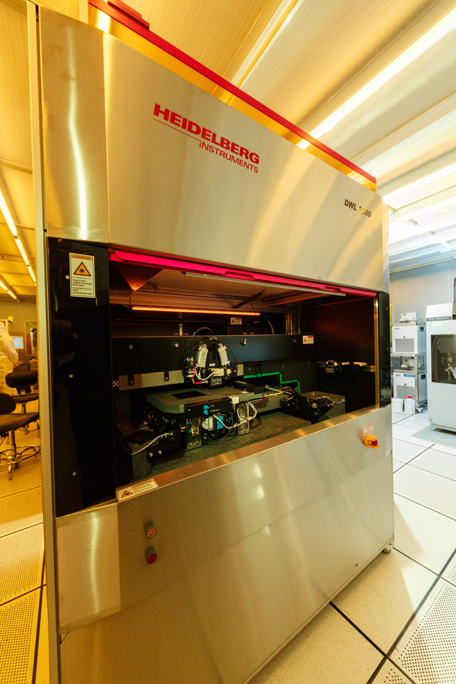
Specifications
1. Environment chamber, providing a stable environment for the system |
||
|---|---|---|
| - Laminar airflow (adjustable): 0.3 – 0.5 m/s | ||
| - Temperature stability: ± 0.1 °C | ||
| - Air quality: Class 10 | ||
2. Stage system with linear motors, air bearings and interferometric position control |
||
| - Maximum substrate size: 9" x 9" | ||
| - Maximum write area: 200 x 200 mm² (min. 5 mm from substrate edge) | ||
| - Substrate thickness: 0 to 7 mm | ||
3. Writing performance |
||
| - Write mode: I and II | ||
| - Minimum feature size: 0.5um , 0.7um | ||
| - Edge roughness(3s): 40nm , 50nm | ||
| - CD uniformity(3s): 60nm , 80nm | ||
| - Alignment measurement accuracy(3s): 60nm, 70nm | ||
| - Overlay accuracy(3s): 160nm, 200nm | ||
| - Write speed (mm2/minute): 29, 110 | ||
JEOL JBX-6300FS E-Beam Lithography System
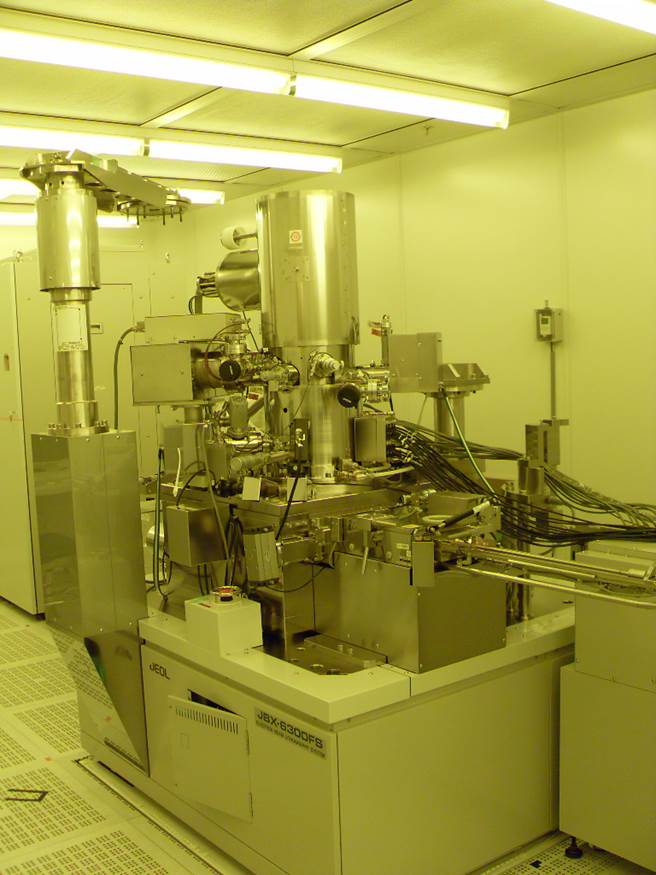
Specifications
| Writing Mode | : | High speed or high precision |
|---|---|---|
| Beam Current | : | 30pA to 20nA |
| Scanning Speed | : | 12M to 250 Hz |
| Accelerate Voltage | : | 20, 50 or 100 kV |
| Max. Field Size (um2) | : | High speed mode: 2000 (20kV), 1000 (50kV) or 500 (100kV); High precision mode: 250 (20kV), 125 (50kV) or 62.5 (100kV) |
| Mask | : | 5” x 5” x 0.09” |
| Wafer | : | 4” or 2” |
| Nano-imprint Mask | : | 65mm x 65mm x 6.35mm |
| Chip Sample | : | 2cm x 2cm, 1.5cm x 1.5cm or 1cm x 1cm |